The electronics industry is going through a huge advancement, and with them, every second updated version is becoming more sleeker and more complex. Did you notice it too? Lately, to grab the opportunities and to meet growing demands, engineers are trying to shift to the SMT PCB Assembly process, besides better manufacturing methods, after seeing PCBs attached to several electronic devices, especially mobile phones, telecommunication systems, and more. People generally think about how these components can be directly hooked to the boards. If you are still confused, the whole idea revolves around the SMT assembly process.
Before diving into the steps involved, it is necessary to understand how it works and why it has suddenly become a vital part of modern electronics.
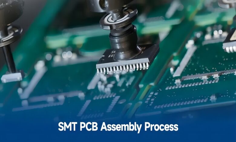
SMT PCB Assembly Process
The Surface Mount Technology (SMT) PCB assembly process is both simple and complex. It involves placing a set of components onto the direct surface of the PCB or printed circuit board. If you are confusing this process with the old plated through-hole assembly, you need to think again! It is completely different from this method: in this method, pre-drilled holes are made, and pins are attached to secure them to the PCB, whereas SMT doesn’t require any pre-drilling. The latter process is more accurate, efficient, and well-suited to match the requirement to assemble electronic components.
7 Simple Steps Involved in the SMT PCB Assembly Process
The process involved here is simple but requires the finest efficiency.
Inspection Of Material
Whenever dealing with electronics, it becomes essential to inspect every material involved. With the help of BOM, or bills of materials, every item should be double-checked with the mentioned shape, size, and even the package type. Even SMDs and PCB parts should also undergo similar changes. One needs to ensure that the PCB employed is not deformed and is free of oxidation for sure. Any negligence may invite unwanted accidents.
Pre-hand Arrangements Before SMT Assembly
If you think the work ends at the inspection, you are mistaken. It is just the beginning. The preparation process involved is too systematic and efficient.
- Start by preparing stencils so that solder paste application can be processed.
- Moisture has to be completely removed from the PCB and BGA chips. One needs to bake these chips for the same.
- The pick-and-place file process for component placement is the next mandatory step.
- Feeders and all the available equipment need to be rechecked to confirm they will work efficiently during the process.
All the steps here are curated to ensure the smooth functioning of the assembly process.
Processing the Solder Paste
After the above processes, the process of the SMT PCB assembly starts. Using stainless steel stencils, apply solder paste to the PCB pads as you place the PCB on the circuit board. Here, solder paste is printed via stencil holes on the PCB. Often, these stencils are different for different needs.
The stencil holes are made through laser-made holes. After applying the solder paste to the PCB, a thorough inspection is done. It is generally processed through a solder paste printing inspection machine. This helps in learning if the paste applied is accurate or not. If it is up to the mark, the PCB is forwarded towards the SMT production line to take the assembly process ahead.
With the help of a solder paste machine, paste is applied smoothly to the bare PCB. Finally, the assembly process’s consistency and perfection can be claimed through all these processes.
Employing a Pick and Place Machine for Placing Components
With the application of a pick-and-place machine, one can rest assured of accurately positioning components on the solder pads; just remember to buy a high-precision machine.
Do you know that the SMD components are often supplied either in trays or reels? Though one can find loose packages when it comes to prototype assemblies. These components are then placed in these machines. Remember, these machines’ functions are completely dependent on customised software so that the loading process goes smoothly.
With the pre-programmed X and Y coordinates, this machine works and manages to place the SMD components on the PCB smoothly. After component placement is complete, the PCB undergoes the reflow process, during which the first article inspection is conducted by an in-line production engineer. From here, the PCBs are moved to an oven for soldering. The first article inspection here double-checks that components have been placed accurately.
Soldering Components On the PCB
Either vapour-phase soldering or the reflow soldering process is used here. Each method comes with its own set of advantages and applications. Vapour-phase soldering is often advocated for prototype assemblies or where the sensitive components need to be soldered. Here, the PCB needs to be overheated until it reaches the vapour phase, and the solder paste ultimately melts. After melting down and then being cooled, the paste is in a position to securely remain stuck to the PCB.
Reflow soldering works well in the case of mass production. You need to maintain a nitrogen surrounding, and then in this controlled chamber, the PCB is placed. The same solder-paste melting process is followed, but using heated air. When the temperature finally reduces, the components get permanent placement onto the PCB. It is the right choice for SMT PCB manufacturing on a large scale.
Complete AOI Inspection
Do you think processing jobs ends here? Indeed, no! To check the flawless execution, additional quality control measures need to be practised. It also involves Automated Optical Inspection, in which several cameras are employed to click high-resolution pictures of the PCB after the soldering process. If it matches with the reference image, it is considered as the selected one or else it is pushed into the defective row. Then it undergoes more stages of inspections, and after final rectification, it is approved. Checking the AOI ensures that the SMT assembly process is accurate.
Visual Inspection
It plays a vital role in checking for minor scratches or any unwanted spots on the PCB surface. This final step ensures that every product here is of high quality in terms of look and functionality.
Wrapping Up
Every single step involved in the SMT PCB assembly process is important, and overlooking any of them may act as a hindrance to the overall quality of the process.